Nothing left to chance
Testing highly complex ETAS hardware during manufacturing
The combination of high circuit board packing density and complex product functionality requires state-of-the-art test methods and an integrated test management system to verify production.
The ongoing development of our hardware products is characterized by two simultaneous trends: rapidly increasing product complexity on the one hand, and the miniaturization of assembled circuit boards on the other. This situation requires the use of modern test methods as well as end-to-end design of the test infrastructure in the product engineering process.
One of ETAS’ core competences is the development of high-performance hardware products that are designed for widely diverse driving conditions, from the extremely hot and dusty environment of a desert to the extreme cold of the far north. To meet these requirements, we rely on our experienced development departments, our specialized external manufacturing service providers for electronic products, and the departments that form the bridge between these different areas. One of the key pillars of this bridge is the Technical Functions (TEF) department. TEF’s responsibilities include development and maintenance of the test infrastructure as well as global management of test data in the manufacturing process for ETAS hardware products.
What distinguishes the test infrastructure used in the manufacturing of ETAS products?
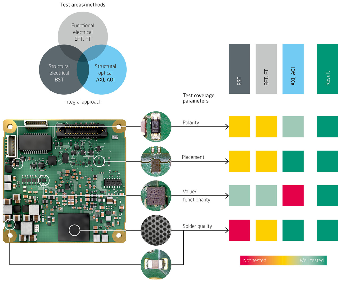
The key to successful test infrastructure design lies in an integral test method approach. This involves weighing various state-of-the-art test methods for each specific product and applying them selectively. A distinction is made between structural electrical, functional electrical, and structural optical test methods. Each test method has its own strengths that can be harnessed for the verification of assembled circuit boards. We distinguish here according to different test coverage parameters polarity, component placement, value/functionality, and solder quality (see Fig. 1).
The structural electrical test
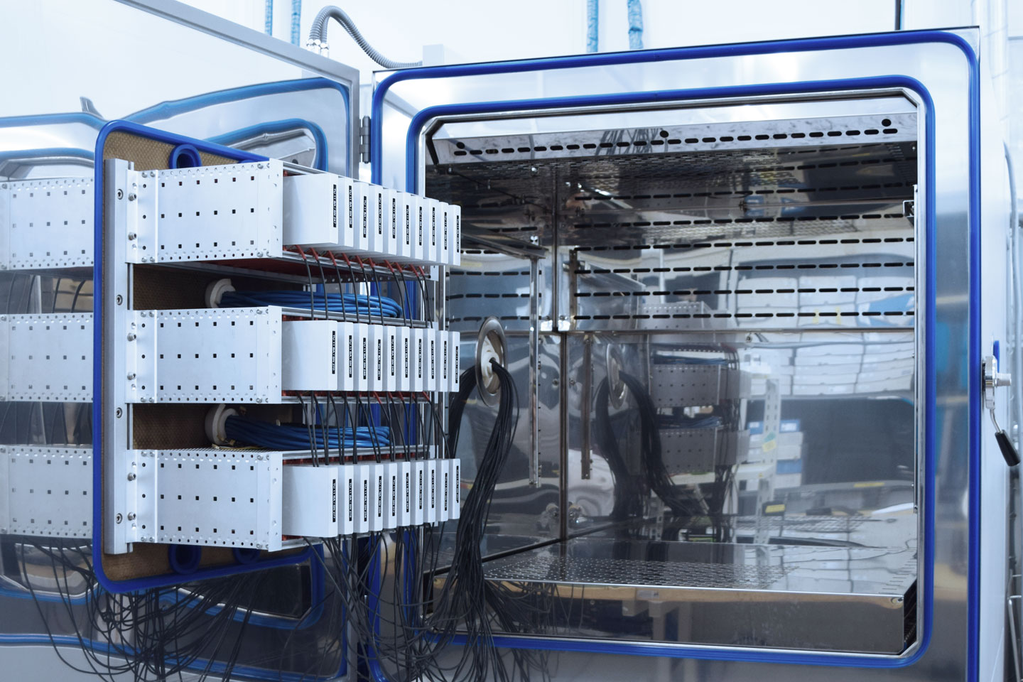
Conventional test methods are reaching their limits due to high packing density, the use of components with connections on the bottom, and extremely small components that appear no bigger than a dot to the human eye. These limits can be overcome by performing embedded board tests using the JTAG (Joint Test Action Group) test bus. This is the boundary-scan test (BST) according to IEEE1149 standard. This test method can be pictured as a kind of “testing worm” that diligently wriggles its way through the circuit board. On its way, it verifies the connections between the components and detects unsoldered connections and short circuits.
The functional electrical test
Two test methods are employed in this area of testing: an embedded functional test (EFT) uses the JTAG bus to access the intelligence of the components that are already assembled. EFTs make use of ChipVORX® and VarioTAP® test technologies as well as test functions programmed in-house in conjunction with the powerful CASCON® systems software from the company GÖPEL electronic GmbH. These high-performance tests detect errors in the dynamic range. This is a key test technology that makes it possible to pinpoint errors with outstanding diagnostics without requiring board-specific software. Functional tests (FTs) with product-specific software are used as a supplement to the EFT. A distinction is made here between cluster testing, which involves in-depth tests of certain areas of hardware, and product function testing, which checks product functionality at the interfaces.
The structural optical test
The key strengths of optical testing lie in the evaluation of solder quality and component placement. It is performed with X-ray systems similar to those used in orthopedics and with state-of-the-art camera systems in 3D image quality. The efficiency of the X-ray test systems (AXI – automated X-ray inspection) and optical test systems (AOI – automatic optical inspection) is therefore of the utmost importance. This area of testing is covered by test systems from our manufacturing service providers. When selecting suppliers, ETAS places great importance on ensuring that manufacturing service providers’ test facilities are suitably well equipped.
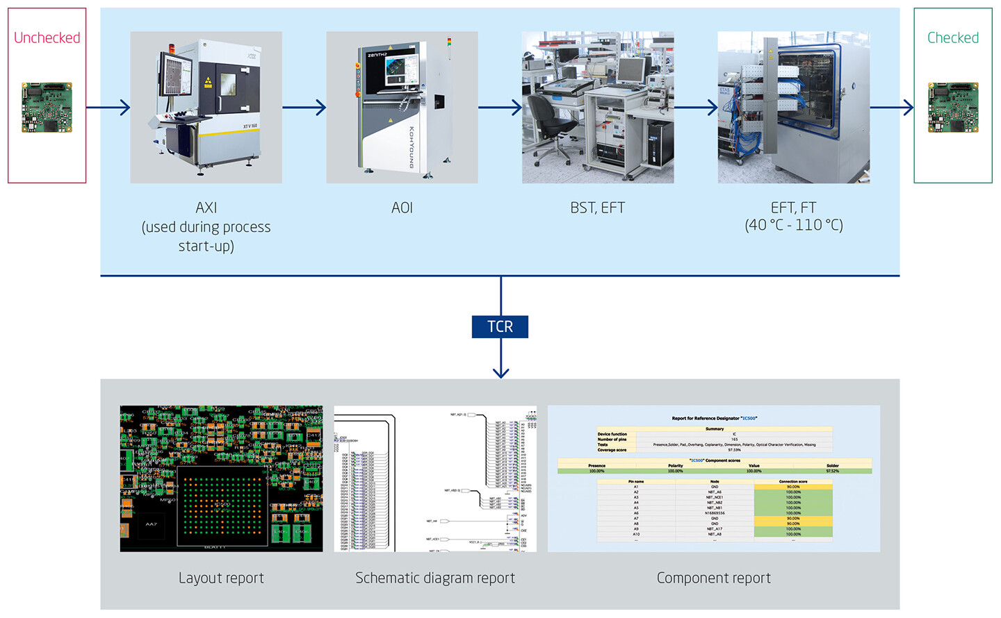
The test chain
The test methods described above are used in highly complex test systems that are embedded in a test chain. Each test system makes an important contribution to product test quality (Fig. 2). Test quality is determined on the basis of test coverage. The test coverage of each individual test system is, in turn, indicated by Test Coverage Reports (TCRs). These reports contain the test coverage parameters of each individual component and component connection, and are used to analyze and optimize the test chain.
The fully integrated test coverage analysis tool TestWay Express® from ASTER Technologies is used to help maximize test coverage and optimize the use of test methods.
Summary
Nothing is left to chance. To accommodate the broad portfolio of ETAS hardware products during manufacturing, we use a modern test infrastructure that has been developed on the basis of state-of-the-art technology. The key to optimizing the testing of our hardware products lies in our many years of experience in developing manufacturing test systems, our use of high-performance, state-of-the-art tools, and our close cooperation with hardware manufacturing service providers. This is an important piece of the puzzle that contributes to the high quality of ETAS products.
Authors
Roland Rothbächer is Senior Manager Technical Functions at ETAS GmbH.
Edip Abay is Development Engineer for manufacturing test systems at ETAS GmbH.
Further information
-
 Nothing left to chance: Testing highly complex ETAS hardware during manufacturing Download